|
#1
 October 7th, 2012, 01:44 PM
| |||
| |||
|
Hy here I am searching for the Visvesvaraya Technological University Logic Design Lab Manual3rd SEM so please can you give me the detail of the Lab Manual and provide me the page where I can download the information of VTU Logic Design Lab Manual 3rd SEM? Visvesvaraya Technological University Logic Design Lab Manual 3rd SEM syllabus or Experimental topics are follows: EXPERIMENT: 1 LOGIC GATES EXPERIMENT: 2 REALIZATION OF A BOOLEAN FUNCTION. EXPERIMENT: 3 ADDERS AND SUBTRACTORS EXPERIMENT: 4 PARALLEL ADDER AND SUBTRACTOR EXPERIMENT: 5 BCD TO EXCESS- 3 CODE CONVERTERS EXPERIMENT: 6 BINARY TO GRAY CODE CONVERTER EXPERIMENT: 7 MULTIPLEXER AND DEMULTIPLEXER  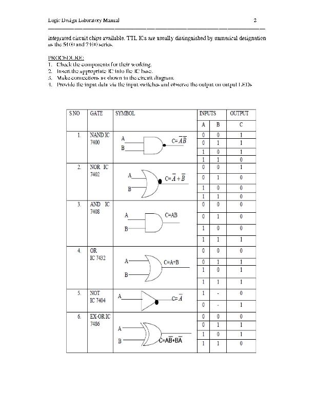       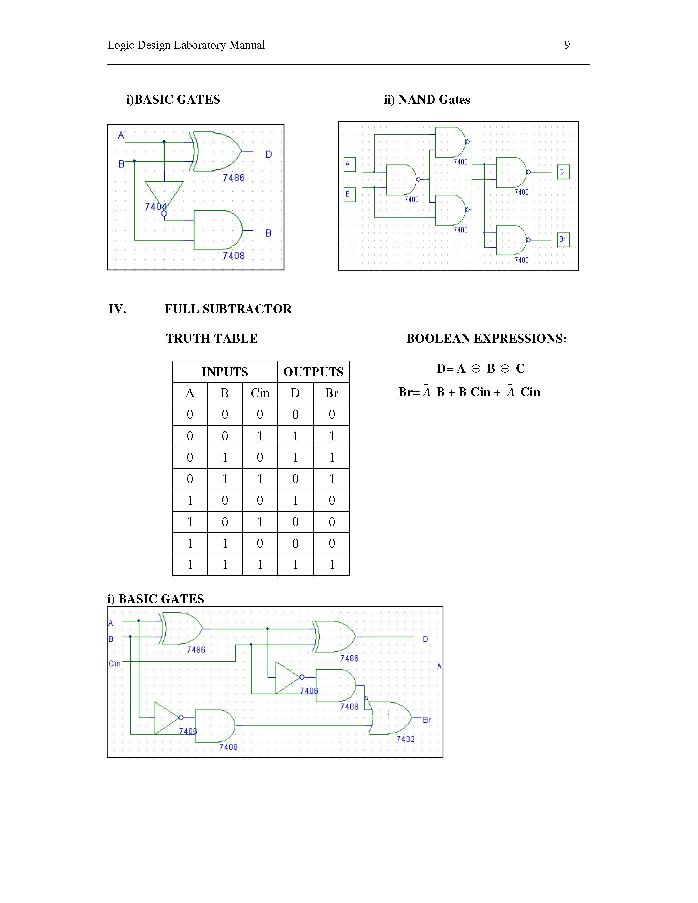  Contact Visvesvaraya Technological University Jnanasangama Machhe, Khanapur Road, Khanapur Road, Machha Industrial Area, Machhe, Belgaum, Karnataka 590014 0831 240 5458 For detailed here is attachment: Last edited by Aakashd; May 21st, 2019 at 10:46 AM.  |
|
#2
October 8th, 2012, 06:25 PM
| |||
| |||
|
As you required VTU Logic Design Lab Manual of 3rd semester so I have mebationed a link here from where you can get it... 4shared.com/file/224619150/a6fdb0ad/LAB_MANUAL__SPICE_SIMULATION_M.html
__________________ Answered By StudyChaCha Member |
|
#3
April 12th, 2014, 02:36 PM
| |||
| |||
|
As per your request here I am providing Logic Design Lab Manual 10ESL38 3rd sem for B.E. Electronics and Communication Engineering of Visvesvaraya Technological University (VTU) Logic Design Lab Manual --- EXPERIMENT: 1 LOGIC GATES AIM: To study and verify the truth table of logic gates LEARNING OBJECTIVE: • Identify various ICs and their specification. COMPONENTS REQUIRED: • Logic gates (IC) trainer kit. • Connecting patch chords. • IC 7400, IC 7408, IC 7432, IC 7406, IC 7402, IC 7404, IC 7486 THEORY: The basic logic gates are the building blocks of more complex logic circuits. These logic gates perform the basic Boolean functions, such as AND, OR, NAND, NOR, Inversion, Exclusive-OR, Exclusive-NOR. Fig. below shows the circuit symbol, Boolean function, and truth. It is seen from the Fig that each gate has one or two binary inputs, A and B, and one binary output, C. The small circle on the output of the circuit symbols designates the logic complement. The AND, OR, NAND, and NOR gates can be extended to have more than two inputs. A gate can be extended to have multiple inputs if the binary operation it represents is commutative and associative. These basic logic gates are implemented as small-scale integrated circuits (SSICs) or as part of more complex medium scale (MSI) or very large-scale (VLSI) integrated circuits. Digital IC gates are classified not only by their logic operation, but also the specific logic-circuit family to which they belong. Each logic family has its own basic electronic circuit upon which more complex digital circuits and functions are developed. The following logic families are the most frequently used. TTL Transistor-transistor logic ECL Emitter-coupled logic MOS Metal-oxide semiconductor CMOS Complementary metal-oxide semiconductor Rest of the detail is attached in below file which is free of cost Address: Visvesvaraya Technological University Jnanasangama Machhe, Khanapur Road, Khanapur Road, Machha Industrial Area, Machhe, Belgaum, Karnataka 590014 0831 240 5458 Map: https://maps.google.co.in/maps?q=vtu...m&z=16&iwloc=A
__________________ Answered By StudyChaCha Member |
|
#4
October 28th, 2014, 07:33 AM
| |||
| |||
|
I need experiment videos of ec and ld experiment! Could you please help me?
|
|
#5
August 19th, 2015, 05:55 PM
| |||
| |||
|
thanks but i need all experiments to download plz get full logic designe vtu lab manual |
|
#6
October 15th, 2015, 12:37 PM
| |||
| |||
|
I need logic design manual of experiment 8,9 & 10 |
|
#7
August 21st, 2019, 11:50 AM
| |||
| |||
|
Can you provide me the Logic Design Laboratory Manual for B Tech 3rd Sem ECE (Electronics & Communication Engineering) Program of VTU (Visvesvaraya Technological University)?
|
|
#8
August 21st, 2019, 11:53 AM
| |||
| |||
|
The Logic Design Laboratory Manual for B Tech 3rd Sem ECE (Electronics & Communication Engineering) Program of VTU (Visvesvaraya Technological University) is as follows: EXPERIMENT: 1 LOGIC GATES AIM: To study and verify the truth table of logic gates LEARNING OBJECTIVE: Identify various ICs and their specification. COMPONENTS REQUIRED: Logic gates (IC) trainer kit. Connecting patch chords. IC 7400, IC 7408, IC 7432, IC 7406, IC 7402, IC 7404, IC 7486 THEORY: The basic logic gates are the building blocks of more complex logic circuits. These logic gates perform the basic Boolean functions, such as AND, OR, NAND, NOR, Inversion, Exclusive-OR, Exclusive-NOR. Fig. below shows the circuit symbol, Boolean function, and truth. It is seen from the Fig that each gate has one or two binary inputs, A and B, and one binary output, C. The small circle on the output of the circuit symbols designates the logic complement. The AND, OR, NAND, and NOR gates can be extended to have more than two inputs. A gate can be extended to have multiple inputs if the binary operation it represents is commutative and associative. These basic logic gates are implemented as small-scale integrated circuits (SSICs) or as part of more complex medium scale (MSI) or very large-scale (VLSI) integrated circuits. Digital IC gates are classified not only by their logic operation, but also the specific logic-circuit family to which they belong. Each logic family has its own basic electronic circuit upon which more complex digital circuits and functions are developed. The following logic families are the most frequently used. TTL Transistor-transistor logic ECL Emitter-coupled logic MOS Metal-oxide semiconductor CMOS Complementary metal-oxide semiconductor TTL and ECL are based upon bipolar transistors. TTL has a well-established popularity among logic families. ECL is used only in systems requiring high-speed operation. MOS and CMOS, are based on field effect transistors. They are widely used in large scale integrated circuits because of their high component density and relatively low power consumption. CMOS logic consumes far less power than MOS logic. There are various commercial integrated circuit chips available. TTL ICs are usually distinguished by numerical designation as the 5400 and 7400 series. PROCEDURE: 1. Check the components for their working. 2. Insert the appropriate IC into the IC base. 3. Make connections as shown in the circuit diagram. 4. Provide the input data via the input switches and observe the output on output LEDs Logic Design Laboratory Manual for B Tech 3rd Sem ECE VTU  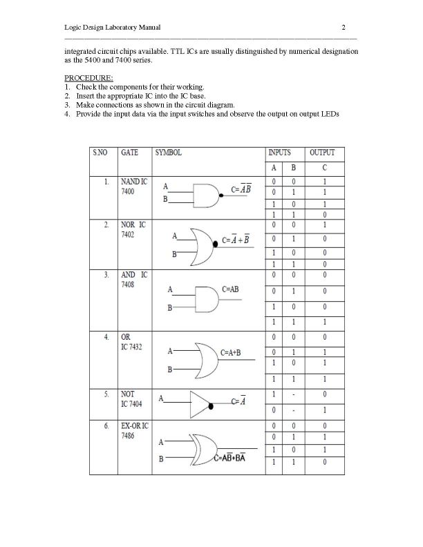  
__________________ Answered By StudyChaCha Member |
 |
| |


