|
#1
 June 8th, 2014, 12:38 PM
| |||
| |||
|
Will you please provide me the Mumbai University, BE in Electronics and Telecommunication, 4th Sem., Electronic Devices and Circuits-II Exam Previous Years Question Papers???
 |
|
#2
June 8th, 2014, 03:24 PM
| |||
| |||
|
This is the Mumbai University, BE in Electronics and Telecommunication, 4th Sem., Electronic Devices and Circuits-II Exam Previous Years Question Papers: 7. Write short notes on any four :- (a) Cascode Amplifier (b) Ideal characteristics of Opamp (c) Role of Level shifter circuit in Opamp (d) Crystal oscillator (e) Opamp as a Integrator. 5. (a) Derive the expression for frequency of RC phase shift oscillator using BJT. (b) Design Op-amp based Wein-bridge oscillator which generates 10KHz frequency. 6. (a) Derive an expression for the Differential voltage gain and differential input resistance of a dual input balanced output differential amplifier. MU BE in E&T, 4th Sem., Electronic Devices and Circuits-II Exam Paper 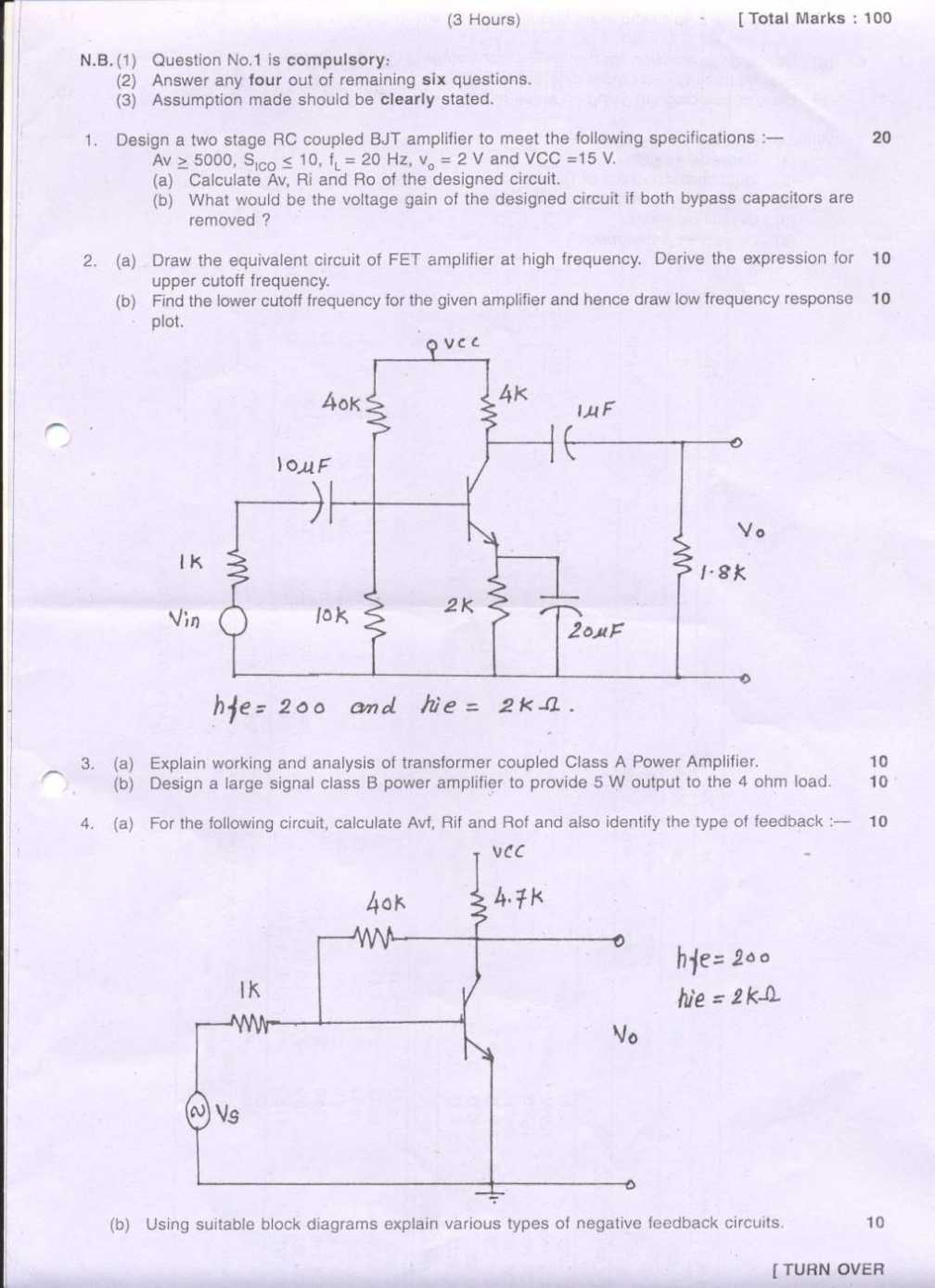 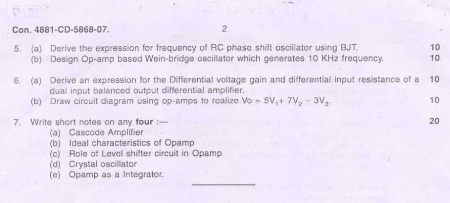  Address University of Mumbai Kalina,Santacruz, Mumbai, Maharashtra 400098, India +91 22 2654 3000
__________________ Answered By StudyChaCha Member |
|
#3
October 12th, 2015, 03:02 PM
| |||
| |||
|
hii, sir I wanted to get the question paper of mumbai university of B.tech E&T, 4th Sem., Electronic Devices and Circuits-II Exam Papers , please provide me the question paper?
|
|
#4
October 12th, 2015, 03:05 PM
| |||
| |||
|
As you asking for the question paper of mumbai university of B.tech E&T, 4th Sem., Electronic Devices and Circuits-II Exam Paper, here I am providing you the question paper of the B.tech E&T, 4th Sem., Electronic Devices and Circuits-II the questions are: 1. Design the two stage R-C coupled CS amplifier to meet the following specifications. 20 IAvl > 100. FL < 20 Hz Va = 4 V. IOSQ= 1.2 mA Ass~me gmo = 5000 ~H Vp= 4V. Assume suitable VDD (a) Design a large signal transformer coupled 'class A power amplifier to 10 provide 10W output to .the 4 Q load. h (b) Explain working and analyze class B power amplifier. 3. (a) Draw the circuit diagram using op-amps to realize Va = 6V1 + 3 V2- 3V3' 10 Derive output expression. (b) Designop-ampbasedWein-Bridgeoscillatorwhichgenerates15KHzfrequency. 10 4. (a) Draw equivalent circuit of FET amplifier at high frequency for the given 10 amplifier and hence draw low frequency response. (b) What are the various methods to improve CMR~ of differential amplifier? 5. (a) Draw BiFET, BiMOS differential amplifier circuits. State application for ~ach. 10 (b) Using suitable block diagrams explain various types of negative feedback 10 ~ circuits. 6. (a) Draw the c circuit diagram of a temper~ture compensated log amplifier. 10 Derive expression of putput. ',. . (b) What are advantages of crystal oscillator over other high and low frequency 10 oscillator. 7. Write a short notes :- (a) Cascode Amplifier (b) Darlington Pair Amplifier (c) Tuned Collector Oscillator (d) Design of Heat Sink. question paper of BE in E&T, 4th Sem., Electronic Devices and Circuits-II 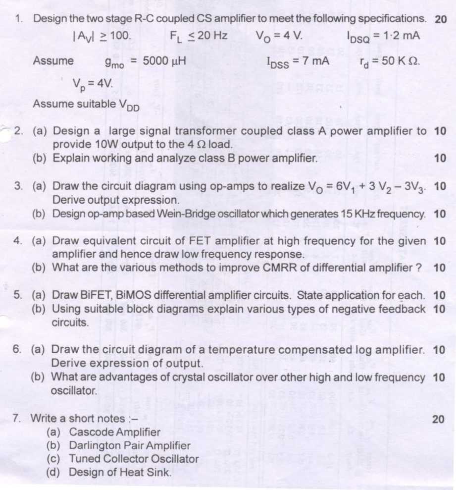 
__________________ Answered By StudyChaCha Member |
 |
| |


