|
#11
 August 21st, 2019, 08:59 AM
| |||
| |||
|
The syllabus of M.E (ElectronicsDigital Systems) Program offered by Savitribai Phule Pune University is as follows: M.E (ElectronicsDigital Systems) SEMESTER-I 504101 Analog & Digital CMOS Design Module I : (8Hrs.) MOSFET equivalent circuits and analysis, CMOS Technologies, Layout Design Rules: Design Rules Background, Scribe Line and Other Structures, MOSIS Scalable CMOS Design Rules, Micron Design Rules. CMOS Process Enhancements: Transistors, Interconnect, Circuit Elements, Beyond Conventional CMOS, CMOS Fabrication and layout: Inverter Cross-section , Fabrication Process, Stick Diagrams. Module II  8Hrs.) 8Hrs.)Static, dynamic and short circuit power dissipations; Propagation delay; Power delay product, Fan in, fan out and dependencies. Delay Estimation: RC Delay Models, Linear Delay Model, Logical Effort, Parasitic Delay. Logical Effort and Transistor Sizing: Delay in a Logic Gate, Delay in Multistage Logic Networks, Interconnect: Resistance, Capacitance, Delay, Crosstalk, Design Margin. Module III : (8Hrs.) Small-Signal Model for MOS Transistor, Analog CMOS Subcircuits : MOS Switch, MOS Diode, Current Sinks and Sources, Current mirrors, Current and Voltage Reference, CMOS Amplifiers : CMOS Inverter as an Amplifier, Differential Amplifiers , Cascode Amplifiers , Operational amplifier, Digital to Analog Converters, Switched Capacitors, Analog to Digital Converters, RF Circuits Module IV: (8Hrs.) CMOS Logic: Inverter, NAND Gate, Combinational Logic, NOR Gate, Compound Gates, Pass Transistors and Transmission Gates, Tristates, Multiplexers, Latches and Flip-Flops, Design calculations for combinational logic and active area on chip; Circuit Families: Static CMOS, Ratioed Circuits, Cascode Voltage Switch Logic, Dynamic Circuits, Differential Circuits, Sense Amplifier Circuits, BiCMOS Circuits, Low Power Logic Design, Comparison of Circuit Families. References 1. Neil Weste and Kamaran, Principles of CMOS VLSI Design, Education Asia. 2. J. M. Rabaey, A. Chandrakasan and B. Nikolic, Digital Integrated Circuits : A Design Perspective, Pearson (Low Price Edition) 3. S-M. Kang and Y. Leblebici, CMOS Digital Integrated Circuits : Analysis and Design, Third Edition, McGraw-Hill 4. P. E. Allen and D. R. Holberg, CMOS Analog Circuit Design, Second Edition, Oxford University Press 5. B. Razavi, Design of Analog CMOS Integrated Circuits, McGraw-Hill 6. P. Gray, P. J. Hurst, S. H. Lewis and R. Meyer, Analysis and Design of Analog Integrated Circuits, Fourth Edition,Wiley, 2001. (Low Price Edition) Laboratory Assignments/Experiments: 1. To implement three input NAND gate using static CMOS logic and draw the Layout for the same. 2. To implement the CMOS inverter using Static CMOS logic and find the impact of W/L on propagation delay and Power Dissipation. 3. Design and Implement Differential amplifier by using AIMSPICE. Analyze the circuit using DC Analysis and Transient analysis. 4. Design and Implement Cascade amplifier by using AIMSPICE. Adjust the W/L ratio and Plot the effect of W/L ratio on Output voltage. Syllabus M.E (ElectronicsDigital Systems) Savitribai Phule Pune University 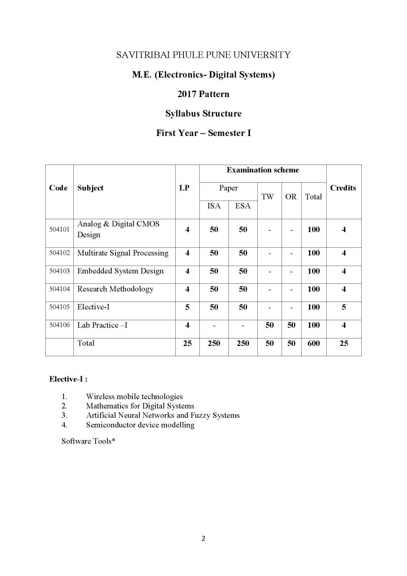   
__________________ Answered By StudyChaCha Member  |
 |
| |


