|
#1
| |||
| |||
|
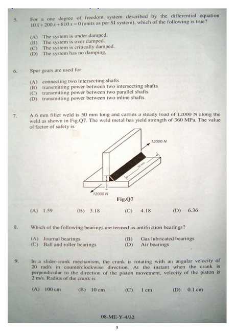
Hello sir, I want some previous year question papers for DRDO exam preparation. Is there any one can provide me here DRDO previous year question paper?
|
|
#2
| |||
| |||
|
Defense Research and Development Organization was established in 1958. DRDO is functioning under Ministry of Defense and Research and Development. Every year DRDO will hire capable candidates for different positions. DRDO CEPTAM Syllabus is given for the candidates. Defence Research & Development Organisation syllabus consisting Reasoning, Quantitative Aptitude, General English, and General Knowledge. DRDO CEPTAM Exam Pattern General Studies English Reasoning Quantitative Aptitude   DRDO Paper On 7th September: Section- A 1.The current I in the given network. a) 1A b) 3A c) 5A d) 7A 2.For the Delta- Wye transformation in given figure, the value of the resistance R is. a) 1/3 ohms b) 2/3 ohms c) 3/2 ohms d) 3 ohms 3.In the given network, the Thevenin’s equivalent as seen by the load resistance Rl is a) V=10 V, R= 2ohms b) V=10V, R=3 ohms c) V=15V, R= 2ohms d) V=15V, R=3 ohms 4.The current I in a series R-L circuit with R=10 ohms and L=20mH is given by i=2sin500t A. If v is the voltage across the R-L combination then i a) lags v by 45 degree b) is in-phase with v c) leads v by 45 d) lags v by 90 5.In thr given network, the mesh current I and the input impedance seen by the 50 V source, respectively, are a) 125/13 A and 11/8 ohms b) 150/13 A and 13/8 ohms c) 150/13 A and 11/8 ohms d) 125/13 A and 13/8 ohms 6.A voltage sourcehaving a source impedance Z = R + jX can deliver maximum Average power to a load impedance Z, when a) Z = R + jX b) Z = R c) Z = jX d) Z = R –jX 7.In the given circuit, the switch S is closed at t=0. Assuming that there is no initial Charge in the capacitor, the current i(t) for t>0 is a) V/R e^ (-2t/RC) b) V/R e^ (-t/RC) c) V/2R e^ (-2t/RC) d) V/2R e^ (-t/RC) 8.For the circuit in given figure, if e(t) is a ramp signal, the steady state value of the Output voltage v(t) is a) 0 b) LC c) R/L d) RC 9.For the series RLC circuit in given figure, if w=1000 rad/sec, then the current I (in Amperes) is a) 2 ∟-15 b) 2 ∟15 c) √2∟-15 d) √2∟15 10.The Y-parameter matrix (mA/V) of the two-port given network is a) [2 -1 -1 2] b) [2 1 -1 2] c) [1 -2 -1 2] d) [2 1 1 2] 11.The maximum number of trees of the given graph is a) 16 b) 25 c) 100 d) 125 12.Given figure shows a graph and one of its trees. Corresponding to the tree, the group of branches that CAN NOT constitute a fundamental cut set is a) 1,2,3 b) 1,4,6,8,3 c) 5,6,8,3 d) 4,6,7,3 13.The Y-parameter matrix of a network is given by Y=[1 1 -1 1] A/V. The Z11 parameter of the same network is a) 1⁄2 ohms b) 1/√2 ohms c) 1 ohms d) 2 ohms 14.For the given circuit, the switch was kept closed for a long time before opening it at t=0. The voltage v(0+) isa) -10 V b) -1 V c) 0V d) 10 V 15.The input impedance of a series RLC circuit operating at frequency W=√2w, w being the resonant frequency, is a) R-j(wL/√2) ohms b) R+j(wL/√2) ohms c) R-j√2wL ohms d) R-j√2wL ohms 16.The threshold voltage V is negative for a) an n-channel enhancement MOSFET b) an n-channel depletion MOSFET c) an p-channel depletion MOSFET d) an p-channel JFET 17.At a given temperature, a semiconductor with intrinsic carrier concentration ni= 10 ^ 16 / m^3 is doped with a donor dopant of concentration Nd = 10 ^ 26 /m^3. Temperature remaining the same, the hole concentration in the doped semiconductor is a) 10 ^ 26 /m^3 b) 10 ^ 16 /m^3 c) 10 ^ 14 /m^3 d) 10 ^ 6 /m^3} 18.At room temperature, the diffusion and drift constants for holes in a P-type semiconductor were measured to be Dp = 10 cm^2/s and μp = 1200 cm^2/V-s, respectively. If the diffusion constant of electrons in an N-type semiconductor at the same temperature is Dn = 20 cm^2/s, the drift constant for electrons in it is a) μn = 2400 cm^2/V-s b) μn = 1200 cm^2/V-s c) μn = 1000 cm^2/V-s d) μn = 600 cm^2/V-s 19.A common LED is made up of a) intrinsic semiconductor b) direct semiconductor c) degenerate semiconductor d) indirect semiconductor 20.When operating as a voltage regulator, the breakdown in a Zener diode occurs due to the a) tunneling effect b) avalanche breakdown c) impact ionization d) excess heating of the junction.
__________________ Answered By StudyChaCha Member |